
A gentle introduction to digital logic design for software developers via HLS

ANNOUNCEMENT: Now you can access an FPGA LAB environment on demand with chiprentals. This service is currently in the Beta stage and is being provided for free. Go perform your projects in a real world environment. Book your slot here. The PYNQ-Z2 board being offered currently is the best choice for trying out ML and AI acceleration projects as well as traditional FPGA development.
Even after we've managed to squeeze out every bit of performance out of our algorithms, there are so many problems today that suffer from being excessively compute heavy. With Moore's law slowly dying, heterogenous computing is rapidly gaining ground in the tech circles where extra-ordinary performance is of paramount importance. Be it AI/ML, Genome Sequencing or even Cryptocurrency Mining, everybody's trying to create specialized hardware that can perform these tasks far more efficiently that the state of the art processors. However, the world of hardware has not been very friendly to everyone mostly due to the fact that it is so different from the usual programming that we're used to. This article aims to demystify some of that stuff.
If you're reading this article you're probably fit into one of these two categories.
a. You're a software developer curious about FPGAs or hardware acceleration of algorithms and yet, the first time you read about HDLs, learned about a clock and the fact that 'always blocks' in Verilog are essentially infinite loops (in some sense), it scared the shit out of you. So you're here trying to find a bridge between your world of sequential programming languages, and the wild territory of fundamentally parallel digital design.
b. You're a practicing digital designer or an FPGA engineer who's been hearing about this thing called HLS and yet never seen someone use it fruitfully in an industry setting, so you're curious about what this tool might be.
If you don't fit into one of the above two categories and you're a beginner to the world of digital design, although this article will teach you a lot of the considerations that go into a hardware design I strongly suggest you work on your HDL skills, you need to get accustomed to the thought process that goes into hardware design and the practices used in the industry. Don't fall into the 'Write code in C/Python/

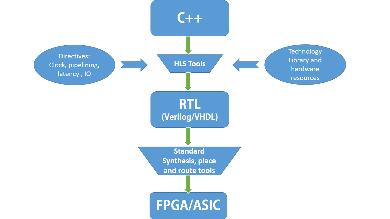
For the software folks, one important thing to understand is that for the longest while, Digital Hardware has been designed using something called a Hardware Description Language. Although it looks and feels like another programming language, it is not. The fundamental mental model required for using a HDL is different from that for a programming language. Think of it like painting a digital logic circuit, except instead of using a brush, you're using a keyboard. The different blocks of code get transformed into real physical logic circuits in hardware.
HDLs can be used to write hardware in a few different ways, but the most popular in is the Register transfer Level (RTL) code that allows one to describe the computation at an abstract level and the tools infer the appropriate hardware.
However, there has been an idea lurking around in this industry that aims to bend programming languages in a way that allows tools to 'infer' digital hardware from code written in a regular programming language. This is called High Level Synthesis or HLS. It's simply an abstraction level above HDL's built with the aim of making digital design more accessible to those with lesser domain knowledge of this field and other software folks.
Let's dig deeper into this world...
The Mental Model:
a. Programming Language - Code block A is written before Code block B and hence it shall be executed first. Whatever changes block A makes to the environment (variables etc ) may have an effect on the functioning of block B because it comes later in time. The compiler is going to convert this code into assembly instructions and execute it on the target CPU.
b. Hardware Description Language (HDL) - Code block A and Code block B describe two separate pieces of hardware, both of which will be present in the end result and shall be operating parallelly in time. They may or may not interact with one another but the fact that block A is written before block B holds no importance whatsoever. Also, this hardware is assumed to keep functioning indefinitely as long as its powered on and the clock signal is toggling (in a way, it's an infinite loop).
c. High Level Synthesis (HLS) - The code is written in a sequential sense, just like in a programming language, yet the compiler (and the synthesizer) is going to 'infer' hardware capable of implementing the functionality presented by this code, the exact hardware that is inferred, and the kind of building blocks it uses, can be controlled by the plethora of directives this tool allows us to use. These directives let you control what you mean by a line of code.
- The unspoken assumption here though, is that you definitely lose a lot of control over your design when you use HLS. Using RTL code still gives you significantly better performance and uses significantly fewer resources in comparison to HLS, but if you need several design iterations before you find a perfect fit for your applications, HLS can boost your productivity immensely. Once you're sure your design works for your application, re-implementing the same design in HDL should give you significant performance boosts over HLS generated hardware.
- That being said, there are a lot of subtle nuances in the way C++ code is written that can mean the difference between mediocre hardware and exceptional performance boosts.
-
Also, there are other ways in which coding for HLS can feel different from a programming language, like...
- The only place you'll every use the main() function is in a testbench where you're calling the design to test it.
- Forget everything you know about dynamic memory allocation because you won't be using it.
- Always try to keep the bounds for your loops fixed and independent of inputs. Vivado hls does have a way to handle variable loop bounds, but the experience is not nice.
I'm not writing this article to teach you HLS, there are other good sources to do that, I just want to explore how this tool makes the developer think as opposed to what an HDL or a programming language does. This is an important thing to explore since it can cause a lot of headaches to developers who are used to a completely different paradigm of thought while programming.
a. Digital hardware runs on a clock

A clock is to a piece of digital hardware what a heartbeat is to living beings. Most digital logic is designed to be synchronized to a clock. There can be asynchronous elements, like signals originating from outside the logic, but by and large the core of the computation is done at the edge(/s) of a clock signal. This scheme keeps everything synchronized and in control.
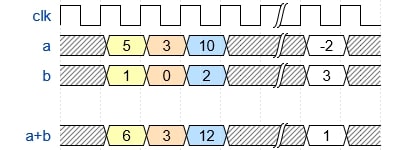
Everything happens at the edge of the clock (here rising edge) in digital logic
An interesting thing to note is that different parts of a design can be running on different clocks. The designer needs to be mindful about any data crossing between two different clock domains and include appropriate circuitry to handle this clock-domain-crossing (CDC).
Programming languages have no concept of a clock. This immediately makes us doubt if synthesizing hardware by trying to bend an inherently sequential programming language is even a good idea. Well....we'll see.
Secondly, Vivado HLS allows you to mention a particular clock period every time you create a new design and beyond that, you have no control over it, meaning this tool has no concept of multiple clock domains, which immediately tells you that it's probably useless for any design of a decent size in the real world since all of them inevitably have multiple clocks working in tandem.
This tells us one thing, HLS is probably not good enough for an entire design, but for a single functional block that works only on one clock, it might still work. In fact, Xilinx docs on this tool suggest that it is targeted towards accelerating the parts of a design that are performing the worst which is to say that we could implement individual functions with this tool and embed these functions in our HDL code which forms the larger design.
i.e implement individual functions (/parts) separately with different clocks as required and later integrate these IPs into the larger design with appropriate Clock-Domain-Crossing (CDC) circuitry.
b. Combinational and Sequential Logic
Digital Hardware consists of broadly consists of two types of elements, Logic gates that perform a certain logical function or computation and Flip-flops that store information.
The Logic gates form what is called the combinational logic. Combinational logic has no need for a clock, logic gates sense the voltage level at their inputs and give a corresponding output after a certain time (called the propagation delay).
The Flip-flops and other combinations of these fundamental memory elements form what is called the sequential Logic. These elements take a clock input apart from the data input and capture the logic level at their data input on every rising (or falling) edge of the clock. A sequential element stores its value until the next clock edge occurs, upon which it updates itself to the latest value at its input at the time of the clock edge.
All of digital hardware you see and use is for the most part made of a combination of Flip-Flops and Logic Gates. While writing RTL code, designers have complete control over what kind of hardware elements each variable or function is mapped into. This knowledge is extremely important, for example when the designers count the amount of delay (no. of clock cycles) any given computation would introduce in the data path.
HLS however, doesn't give you the fine grained control over which type of logic element to use unlike verilog wire and reg variables. Most of the decision making is one by the directives. The tool will always try to minimize the latency for the given clock frequency.
c. Parallel vs. sequential AKA area vs speed
When you run a program on your CPU, it essentially breaks down that computation into a sequence of steps. Even if the computation you're trying to perform is inherently parallel, there is no way the CPU can execute two instructions at the same time. Yes we have lots of special hardware units in today's CPUs meant for operations like vector multiplications, but by and large the parallelization in a general purpose CPU is very low.
However, while designing hardware that is specific to a particular purpose, we can optimize it for any level of parallelization that may be present in our data. Let's take the simple example of an accumulator like so...
//Straightorward vector multiplier with no optimizations (Fully rolled loops)
#include "ap_cint.h"
#include <stdio.h>

#define N 4
int i;

void vector_multiplier(int8 in1[N], int8 in2[N], int16 out[N]){

	MULT:for (i = 0; i < N ; i++){
		out[i] = in1[i]*in2[i];
	}
}
//Performance Metrics:
//Latency: 13 clock cycles
//Utilization: 29 FFs, 98 LUTs
The hardware Inferred by the above sequential code would look something like so...
-d0ae66af10b3d96894f8194c15967a82.png)
HLS allows us to increase parallelism using directives like 'LOOP_UNROLL'. What this does is it schedules operations in parallel whenever possible by duplicating the hardware resources. In principle, if there are no dependencies between different iterations of the loop (i.e the current iteration does not use any of the outputs calculated in the previous iterations), fully unrolling the loop can finish the computation in a single clock cycle. Of course, all of this improvement is at the cost of higher resource utilization.
//Vector Multiplier with the main loop unrolled
#include "ap_cint.h"
#include <stdio.h>

#define N 4
int i;

void vector_multiplier(int8 in1[N], int8 in2[N], int16 out[N]){
	MULT:for (i = 0; i < N ; i++){
#pragma HLS UNROLL       //Notice the pragma that directs the tool to unroll this loop
		out[i] = in1[i]*in2[i];
	}
}
//Pefrormance Metrics:
//Latency: 3 Clock Cycles
//Utilization: 36 FFs, 311 LUTs
The hardware inferred by the optimized code using the LOOP_UNROLL pragma would look something like this...
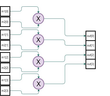
Evidently, the parallel logic above gives you the required result much faster than the sequential one, but at the same time it takes up about N times more resources and thereby area on the chip which may or may not be permissible depending on the overall constraints on the size of the chip. The other option is to use fewer hardware resources and reuse them over different inputs in time, except it would take more clock cycles to complete the same computation. This is a tradeoff that digital designers have to constantly consider.
One more eccentricity of HLS resulting from the nature of hardware is that loops with variable bounds cannot be unrolled. This could be a blocker for those coming from the software background.
d. Latency Vs. Throughput
Imagine a tunnel, now the amount of traffic passing through this tunnel can be expressed in two different ways...
How long does it take a car to go through this tunnel assuming it were empty. This measure depends on the length of the tunnel, speed of the car and perhaps the quality of the roads. This is called Latency of the tunnel.
Another measure of the capacity of this tunnel is 'How many cars can pass through the tunnel per a fixed unit time'. This measure has to do with the width of the tunnel or the number of lanes it supports. This is the throughput of this tunnel.
Replace cars with data and tunnels with computation logic in the above analogy and you get some important performance metrics used to develop digital hardware.
Reducing latency is a non-trivial concept that greatly depends on the design and designer. It is closely tied to the number of different steps the operation has and how many clock cycles is required for each. At first sight, you might say, 'If you want low latency, just use purely combinational logic, so that you get the entire computation done in a single clock cycle.' You'd be correct in saying that, but the big caveat here is that there's only so many levels of combinational logic you can stack up before the propagation delay begins to increase significantly limiting the frequency you can run your design at. Any combinational logic should finish its computation and have its output ready for capture by a Flip-flop within one clock period. This requirement puts a limit on how high the frequency of the clock can be (equivalently, how small the period of the clock can be) due to the largest combinational block in the design.
One popular recipe for building high throughput applications is Pipe-lining. Pipelining is the very concept that distinguished Ford Motor company's assembly lines from the rest. It is the simple yet elegant idea that in a process with multiple steps, each subsequent stage can work on a different input, leading to efficient sharing of the same resources over multiple inputs and thereby increasing the delay between subsequent outputs. Here is the example image of pipelining from Stanford's website... The image says it all
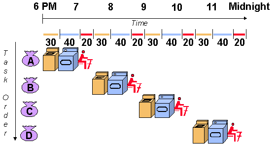
A laundry service with no pipelining implemented
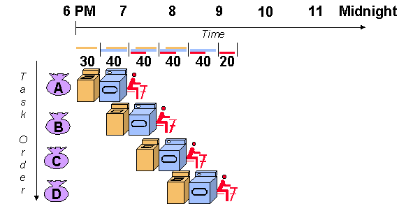
The same laundry service with pipelining implemented, leading to much lower times.
Latency = time it takes for given input to arrive at output
Throughput = rate at each new outputs appear (called Initiation Interval by Vivado HLS)
The tricky part with pipelining though is making sure the logic blocks are not starved of data due to limited memory bandwidth. This can happen due to many reasons like when two operations running in parallel (on different inputs), require data from the same memory in the same clock cycle. It could still work for a dual port memory, but beyond that the pipelining fails and the tool increases the initiation interval to accommodate this limitation.
Another aspect of the pipeline is that the entire pipeline can run only as fast as the slowest sub operation in it. For example, in the laundry service example above, what would happen if the washer took much less time than the dryer? The washer would keep accepting and processing new inputs at a much faster rate than the dryer can keep up. Essentially, the washer has to wait for the dryer to finish before accepting a new input. The basically makes the washer as slow as the dryer (after including the wait time). So the pipeline can only accept new inputs as frequently as the slowest stage can accept new inputs.
HLS, however, abstracts away these details from the programmer, you can choose which loops should be pipelined and also specify the Initial Interval the tool should target, but the exact granularity of it is decided by the tool and the achievable II is reported.
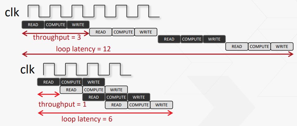
The most popular example of pipelining at the intersection of hardware an software is the pipelined microprocessor architecture. Here, each of the operation forms a stage in the pipeline. To keep things simple, let's look at an example design that performs three simple operations on an incoming stream of data...
//A simple three stage process
#include "ap_cint.h"
#include <stdio.h>
#define N 3

void loop_pipeline(int A[N]) {
#pragma HLS_PIPELINE
  int i,j;
  static int temp1, temp2;
	static int acc;

	LOOP_I:for(i=0; i < 3; i++){
				READ
				COMPUTE
				WRITE
	}
	return acc;
}
Vivado HLS also gives some interesting directives like FLUSH, which prevents the loop from stalling when the input data valid goes low in between and keep working on the values already inside the pipeline.
e. Interfaces
One of the biggest chunks of work while design any piece of hardware is to figure out how data comes in and goes out of the design. Interface performance is often the bottleneck for any design since there are hard physical limits that need to be pushed to make interfaces faster.
Just as the external interfaces matter, each sub-block in our hardware has to choose the appropriate interface to read and write data from and to the logic external to this block. It is very important to use the right kind of interface in order to maximize the performance you get out of your hardware.
Block Level Interfaces:
Let's say there are two independent blocks of hardware that are interacting with each other.
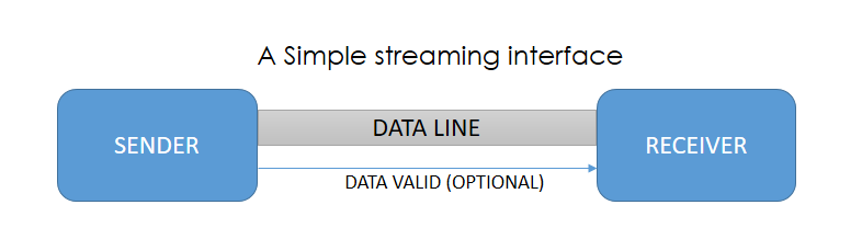
In a typical setting, one block of hardware is feeding data into another. Now two possibilities arise, for one, none of these blocks stall at any point of time. That is, the sender constantly streams data and the receiver constantly accepts data, optionally there might be a couple of other signals indicating when the data is valid etc. This is pretty simple to implement.
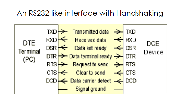
Now consider the case where, one or both of the blocks cannot grantee a constant stream of data but rather they keep processing inputs as they come and the outputs keep flowing forward. In this case, you need some mechanism for the blocks to hardware to tell each other when to stop and when to go. This is often the case when you are interfacing with a block of hardware that you have not designed. You cannot make any assumptions about its internal structure and need a reliable interface that tells you when to feed it data and when to read its outputs. Similarly, the destination block could be a slower piece of hardware compared to the source, in which case it should be able to indicate to the source that it needs more time to finish the currently active process and cannot accept new inputs till then.
This is all done through a handshaking or a flow control mechanism. It adds more signals to the interface between the blocks and ensures reliable communication. These interfaces can be very simple like the flow control enabled UART or very complex like the AXI Full interface for larger blocks.
Vivado HLS gives us a lot of options in this regard. You can select everything from a simple wire-like interface to the most complex AXI interface for a particular I/O port and all the RTL complexity will be handled for you. In fact, the tool will even create test-bench templates that properly match these interfaces automatically, saving you so much time for larger and complex interfaces.
Port Level Interfaces:
After the block-level protocol has been used to start the operation of the block, the port-level IO protocols are used to sequence data into and out of the block.
There are architectures where the data coming into and going out of computational blocks need to be stored in memory, be it a global DRAM or a local Block Ram. This data might be used later be the same block or a different one.
One classic example is a network switch storing the random incoming packets temporarily so that it can re-order them while sending them out further.
RAMs are the most popular kind of elements used for feeding data into a hardware block and also storing its output after the computation.
Block RAMs, which are readily available in FPGAs are commonly inferred by tools when a memory based interface is chosen for a function.
It looks something like below:
Often, the code might imply more than two reads in a single clock cycle, something like so...
void func (int mem[N], int out) {
...
SUM_LOOP:for(i=2;i<N;++i) {
sum += mem[i] + mem[i-1] + mem[i-2]; //three reads to the mem array
...
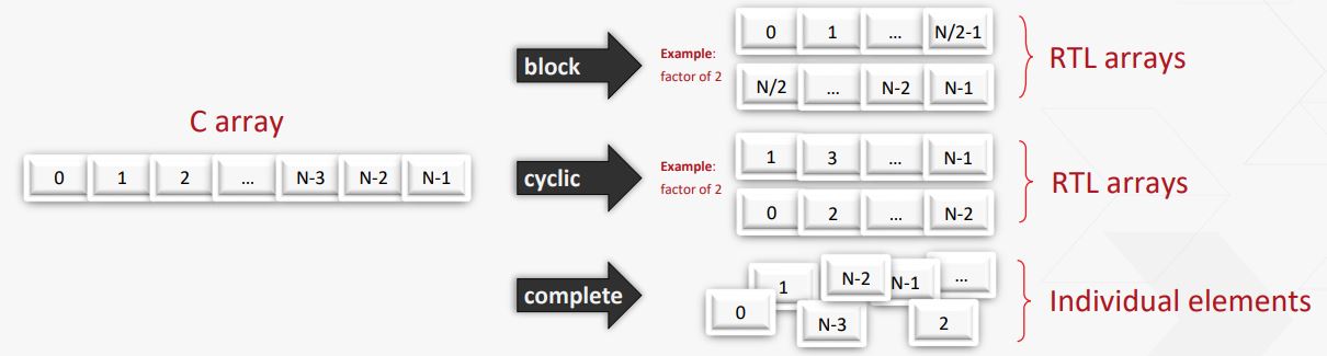
}}Since the 'mem' array is mapped to a RAM, and FPGAs or even most ASIC libraries have only dual port RAMs, this line will limit the throughput of this function. As a workaround to this the 'HLS_ARRAY_PARTITION' pragma will automatically break the 'mem' array into two smaller arrays each with two ports or even further for that matter. Something like so...
FIFOs are another set of elements that are used for anything from buffering data to connecting two pieces of hardware running on asynchronous clocks. They're also useful when the source of the data is erratic and outputs values once in a while. A FIFO between the source and destination can buffer these erractic data blocks into a nice continuous stream of data.
The FIFOs help form an elastic region (like the suspension of a car) that accommodates the differences in number of writes and reads.
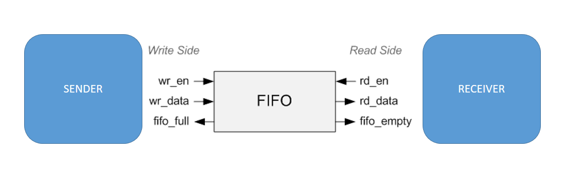
The most common example of using FIFOs are Tx and Rx buffers for generic communication interfaces like UART, SPI where the processing system has no idea when or how frequently the external world is going to sent data in through this interface.
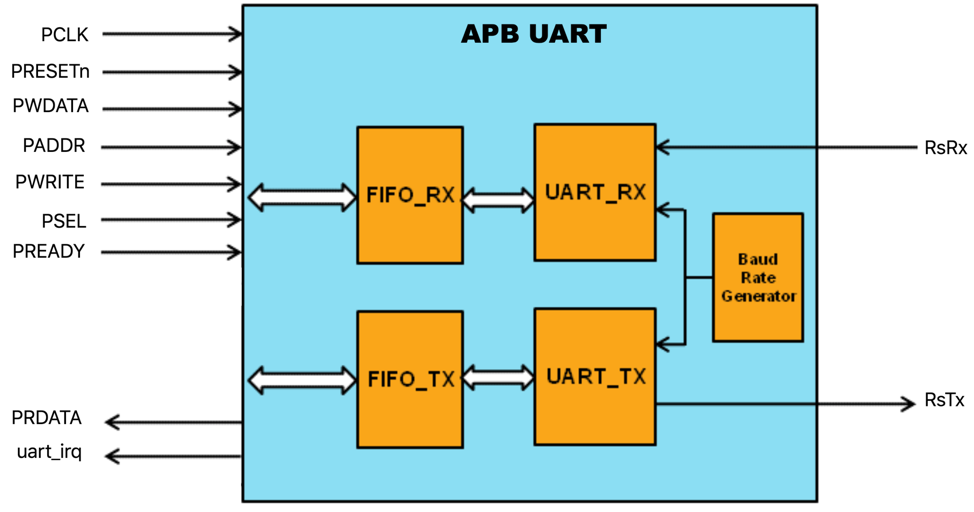
Vivado HLS gives the user lots of options in this regard. Here is an image summarizing all the different interface types that the tool can be made to infer with a simple C++ Pragma.
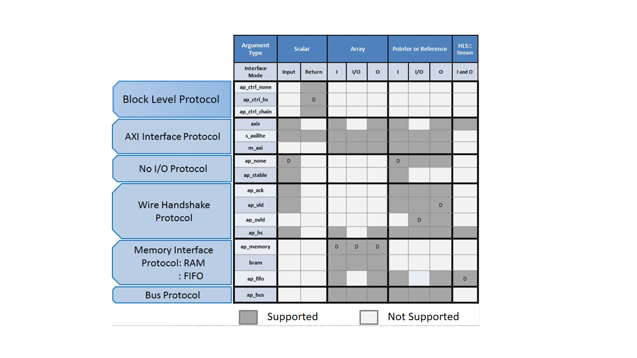
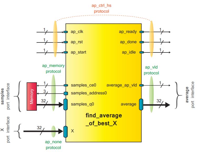
Below is an example of a block of code taken from the Zynq Book
Code for calculating the average of a bunch of stored samples:
void find_average_of_best_X (int *average, int samples[8], int X)
{
 // body of function (statements, sub-function calls, etc.)
}
The interface diagram for this block looks something like this. The upper ports show the block level protocol and the lower ones show the port level protocol selected by the designer for this function.
f. Numbers and Arithmetic: Fixed point vs Floating point representation
Although there are a great number of hardware applications that do not require doing arithmetic operations, it entails a lot of decisions to be made when the need arises. At a fundamental level, hardware has no concept of positive and negative or integral and fractional numbers, these are higher concepts that exist only in our heads. It is the job of the software layers above the hardware to take care of these ideas.
In hardware, bit vectors of different widths is all there is. How you utilize this to implement higher order concepts like fixed point and floating point numbers and the corresponding arithmetic operations is up to us. In applications like DSP where number representation is of great importance, the hardware designer has to take care of the decimal point and quantization so that the Software interpreting its outputs receives data in the expected format.
The choice between fixed and floating point representations for numbers heavily depends on the application scenario. The quantization costs of using a fixed point representation depends on the data being processed. I have written extensively about this in some other posts like this
It turns out though, that implementing even the basic arithmetic operations like addition, multiplication, division etc is very expensive on the resource side when the numbers in question are represented in floating point format.
Fixed point numbers on the other hand, directly map to generic integers when it comes to arithmetic operations, making them much more resource friendly and easy to handle.
This often forces designers to use fixed point arithmetic and use further algorithms and techniques to compensate for the loss in precision. Popularly, the Deep learning world uses high precision floating point data-types for training the algorithms but significantly reduce precision during inferencing to reduce hardware costs and latencies.
This is one area where HLS gives significant productivity boosts over RTL. All the data-types and their arithmetic is reliably handled by the generated RTL and saves a lot of developer time in managing such a basic aspect.
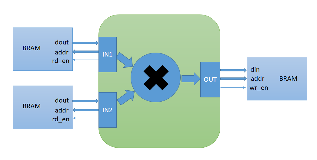
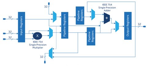
The below image shows a floating point multiplier, compare that with a simple integer multiplier (the X block) in this image.
g. Resource optimization
Optimizing on the amount of logic resources the design uses, is one of the primary considerations while designing hardware just like time and space complexity is for software engineers. Although FPGAs are getting larger and larger with time and designers can sometimes fall back on the extra fabric, in the ASIC industry still needs to squeeze out the maximum performance and use the least number of gates possible.
HLS can be a significant setback in this aspect since the utilization is several times higher in comparison to RTLs. This loss of efficiency could easily be a deal-breaker for a lot of applications.
I look forward to a future where RTL designers can take the code generated by HLS and further optimize it. But given the current structure of these tools where even a simple accumulator requires a big state machine, I don't see this happening soon
A concluding Summary:
HLS technology in general, has been in the development pipeline for the longest time now but has hardly materialized into a paradigm that can transform lives of logic designers. The usual reaction you get when you mention using HLS to a FPGA engineer is something in the lines of...

or...

However, things have come a long way and as it stands now, I am of the opinion that HLS can be a decent addition to one's toolkit if one knows when to use it and when not to. One such case is when you need to try out the acceleration of a particular well defined algorithm that takes a certain defined input to give a certain output while using a single clock. A lot of common algorithms usually implemented in software can be accelerated by parallelizing them with efficient hardware structures.
HLS also significantly benefits on the simulation side since simulating in C++ is thousands of times faster than traditional verilog simulators. If you're an RTL designer, you understand how much time this can save you.
Well here's the thing, people touch FPGAs only when there is an overwhelming requirement for extraordinary performance. For most normal stuff, we have really fast CPUs and for great stuff, we have other things like GPUs and dedicated SOCs etc. The programmers for these things are also quite readily available making it easy on the purse, but when it comes to FPGAs, all of these factors work against you, it takes a lot of time to write good and optimized designs for these devices if you wish to achieve decent acceleration at scale and everything from the engineers to the device expertise itself is not abundantly available owing to the nature of hardware itself. So in short, if someone's investing in dedicated hardware in the form of FPGAs, they expect the best of the best, which and HLS technology is currently far from providing that. But it would be too shortsighted to say that HLS cannot replace HDLs at some point in the future, although that future doesn't seem near.
Finally, thanks to the awesome community r/fpga for all the memes!