
PCB design in altium
I once took a course on PCB design in Altium Designer. I hardly do PCB design in my daily life, but I’d like to be able to do it myself if the need arises. Here are some notes of my learnings that I can come back to. I hope someone else out there finds it useful too.
- Top Layer (red) - Copper. Usually has the pads for components.
- Top Overlay (yellow) - Silkscreen. The print with names and boundaries. The size of the boundary for each component should be according to its dimensions in the component datasheet.
- Top Solder (purple) - The areas that are not covered with green/blue color of the PCB. You need this area around the pads so that they're not covered in the PCB color.
- Top Paste (Grey) - The area covered by tin during the manufacturing process. This layer is used to create the stencil which is a metal/plastic sheet with holes (holes exactly where the top paste layer tells them). They place this sheet on the PCB and apply tin before soldering down the SMD components.
THE ABOVE 4 LAYERS ARE PRESENT BOTH ON THE TOP AND THE BOTTOM SIDE.
In the library, we usually place components and footprints only on the top layers. Later during the PCB layout, we transfer these components to the bottom if necessary.
Reference point - The point used by the pick and place machine during board assembly
- The imported 3D models are being placed on the mechanical 1 layer.
STEPS:
- Make the schematic symbol - placing pins and rectangles or drawing resistors/LEDs.
- Make footprint - making footprint using the above layers
- The 3D model gets placed on the Mechanical 1 layer.
- The Assembly diagram is drawn on the Mechanical 29 layer.
- Draw an outline of the footprint on the mechanical-29 layer. This outline is the same as the silkscreen for that footprint.
- Place a full circle near pin1 of the component inside this outline.
- Place a string (.Designator)
- Connect footprint with the schematic symbol.
- Once all the schematic symbols are made and the corresponding footprints are connected, we have to draw the schematic, where all the components are placed and wires are connected. We usually name schematic symbols with designators like ? which are replaced by numbers, so annotate the schematic to assign numbers to each component.
- Once the schematic is ready, we need to start placing footprints on the PCB, most tools have an option ('design->update PCB document' in Altium) that takes all the footprints of each component in the schematic and places them randomly in the PCB doc and shows wires connecting them according to the connections in the schematic. Now you need to change the PCB size to the exact dimensions required and place each component in the right place in a way that would make it easy to route paths between the connected pins.
- Once all the components are placed, we route the PCB. i.e make each and every connection according to the schematic.
- We Pour the polygons for all the power nets (+5V, +3.3V, GND). This is to be done on both layers. Note- we need to draw a different polygon for each source, eg. +5V and +5v USB are two different power lines. By default, the GND plane has the highest priority of all, so preferably pour all the other polygons first and then pour the GND in the remaining area. Otherwise, go and change the priority.
- In areas where there is not enough space to draw a polygon, change the thickness of the power lines to something high like 1mm.
- Eventually after pouring the polygons, if you have enough space, move the remaining signals far away from each other as much as possible.
- Set the silkscreen layer properly and add the names of some important pins/buttons like RESET etc. in big and bold font. Whatever text you put on the bottom layer should be mirrored.
- Add any company logo etc ( on the top/bottom solder layer)
- Create assembly drawing layer.
- Create a Mechanical drawing layer.
- Create a manufacturing notes layer telling the manufacturer all the specs needed on your PCB.
TOOLS & TRICKS:
- You can add snap points for a particular object in the 2d mode so that it is easy to move it around. for example, add a snap point in the center of the object and use it to place it exactly in the center of the footprint.
-
- and - can be used to jump between layers while using a tool. + jumps to the next layer on the bar at the bottom and - to the previous
- While drawing a schematic, any two nets with the same net name will be automatically connected to each other, you don't have to draw a line connecting them in the schematic, this makes the scheme look better.
- While placing components on the PCB, place the mounting holes first, next place the connectors, next, the MCUs, next, the coupling capacitors, then resistors, etc
- For design rule values, use preferably use the same values as in this course, only things you need to check with your PCB manufacturer are
a. minimum clearance (named clearance in Altium)
b. minimum thread width (named width in Altium)
c. minimum via (named routing via in Altium)
NOTES:
- 0.1uF 0805 cap, 100k 0805 resistor .... - here 0805 is the physical size of the component, and it is ideal for hand soldering.it means, 0.08 inch by 0.05 inch
- For small projects/prototype manufacturing, always select a cut-tape packaging for components.
- While placing pins, the side of the pin with the white square ( in Altium ) is the electrical (exposed) side of the pin, the other side is the side that is inside the component. So the side with the white square should be on the outside since you can connect a wire only to the electrical side of the pin.
- While drawing a capacitor use grid value as 1 mil.
- when in need of dimensions for footprint, search for
'footprint dimensions in millimeters' on google - CHIP-R dimensions are for resistors, MLCC dimensions are for capacitors. Generally, look at the dimensions for reflow soldering.
- While selecting a ferrite bead look for the parameters, max current rating, DC resistance, frequency resp.
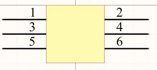
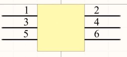
- The following image shows the pin numbering scheme for headers etc. for ICs the order would have been different.
- It is always recommended to connect a 22 or 33-ohm resistor in the path of the clock signal.
- Ideally, we want one entire layer of the PCB to be a ground plane. But that is very hard to do in a 2 layer PCB, so we place the maximum components and routing on the top layer and try our best to make most of the bottom layer a ground plane.
- If the power pin is input, use a bigger decoupling cap (10uf), if it is an output, use a smaller one(100nf).
- While placing LDO or other power distribution circuitry, read the hardware design recommendations, you need to place the capacitors close to the pins to which they're connected.
- In general, the thickness of the dielectric between the layers of the PCB should be 1.6mm
- Preferably do not route reset too close to the clock, if possible use a different layer.
- Do not route close to the mounting hole, route around it.
- [IMP] while routing any differential pair signals (like USB), some specifications are to be met, the simplest of which is to keep them as short as possible and route them very close to each other, others include some standard thread width and impedance. However, it is very hard to meet these specs on a 2 layer PCB. So do the best you can.
- For every power line you route, check how much maximum current could be flowing in that path, the line width should be changed accordingly, similarly, vias also have a maximum current rating. if necessary you need to place two vias next to each other if one is not satisfying the current requirement. (the max. current from a USB power pin is 1.8A).
- Altium will not auto-optimize away the locked components. This is useful for some things like placing multiple vias next to each other due to current limitations.
- For larger and complicated PCBs first start with the most important interfaces (like BGA, memory, etc.) and also place all the vias first and route later.
- After pouring polygons, if there is a via on a major power line(+5v), place multiple vias next to each other.